Recent technological advances in the development of flash memory based devices are consolidating their leadership position as the preferred storage media in embedded systems at the enterprise-scale as well as in end user storage systems. Unlike hard disks, flash devices are free of any mechanical moving parts. Thye have no seek or rotational latency and consume significantly less power. However, the internal design of flash technology make its performance highly dependent on workload characteristics provided by the Flash Translation Layer (FTL). The design of the FTL which basically performs virtual-to-physical address translations and hides “bad blocks” or the “erase-before-write” characteristics of flash. Our previous article was all about Flash File Systems, this time we write more about the Flash Translation Layer.
Flash Translation Layer

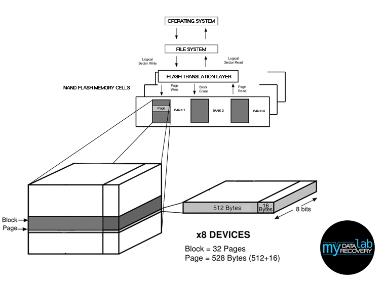
The Diagram above shows a standard flash translation layer that allows an array of NAND flash to be addressed as a set of standard 512Byte logical sectors. In the real world these values are usually multiplied giving 1K, 2K, 4K or 8K logical sectors. To allow a higher-level system, such as a file system to use NAND flash effectively it is necessary to use an FTL that carefully manages the flash while providing a simple logical sector interface to the host system.
NAND flash memory is a very cost effective flash storage medium. However, it has certain characteristics that prevent its use as a simple continuous storage array. It may contain bad blocks; bad bits may develop in previously good blocks; and heavily used blocks will “wear-out”.
Key Features of Flash Translation Layer are:
- Page to Block Management
- High performance
- Zero copy block read/write
- Cache options
- Safe from unexpected reset
- Effective wear-leveling algorithm
- Bad block management
- Automatic garbage collection
- Small code footprint
- Small RAM usage
- Sample drivers and ECC algorithms
- Fast initialization
- Fail-Safe
FTL is designed and tested to handle unexpected system resets cleanly. If a write is initiated during a system reset, and not completed, then the old state of the logical sector being addressed will be presented on start-up. If the write operation was complete, then the new state of the logical sector will be read. No in-between states or complex recovery procedures are required.
All flash devices suffer from wear, since the repeated use of a particular area of flash increases the likelihood that it will fail. Distributing the usage of blocks across the whole flash array greatly increases the lifetime of NAND devices, but effective wear-leveling is a complex task. Seemingly “obvious” algorithms tend to fail in real-world testing. Therefore, sophisticated wear algorithms (both static and dynamic) have been developed that are tune-able to specific systems needs. These ensure that all the blocks in a NAND flash array are evenly written to within a configurable set of specified parameters.
Basic Algorithms
There are many solutions for the algorithm design of the Flash Translation Layer. The following are a few of the most well known options:
TrueFFS
Depite the name, True flash file system or TrueFFS are designed to run on a raw solid-state drive, not common to most modern consumer SSDs. TrueFFS implements error correction, bad block re-mapping and wear leveling.TrueFFS was created by M-Systems and acquired by Sandisk in 2006.
ExtremeFFS
ExtremeFFS is a another technology developed by SanDisk. It allows for an improved random write performance in flash memory compared to traditional systems such as TrueFFS. Sandisk claims the technology improves random access speed in solid-state drives by a factor of close to a 100. It can be found on multi-level cell implementation of NAND flash memory. A version of TrueFFS, called TFFS or TFFS-lite, is used in the VxWorks operating system.
Various Solutions
Most present day flash devices including monolithic ones use some variation of FFS. Designing an FTL for a flash memory manufacturer is a well paid job and programmers continue to seek varied solutions to achieve the best performance. This means that there are many different ideas on ways to increase full performance. In these cases Specs are often hidden or not made available to public.
Conclusion
NAND data recovery, as we outlined in previous articles, is based on reverse engineering (cracking the code, so to speak) or getting specs from the manufacturers (aka-social engineering to those in the hacking world).
We are dedicated to knowing how these things work and believe in sharing our knowledge with all who are interested. To learn more read recently published paper NAND Flash Data Recovery Cookbook.
My Data Recovery Lab is committed to research that leads to successful recovery of data, regardless of the data storage device. This certainly includes digital storage devices based on NAND Flash Memory.

